If you look through datasheets you will find a strange circuit used in front of some ADCs. It looks like a low-pass filter, but you will not find this topology in books.
Let’s try to figure out what it is, how it works and how to design it.
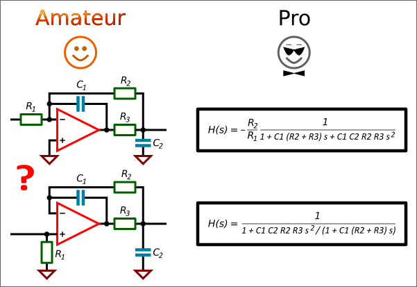
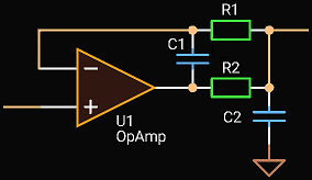
Transfer function
Assuming ideal Op Amp, write a transfer function of this circuit.
 |
| «In-The-Loop» 2-nd order low-pass filter |
         R2                     1
H(s) = ? —— —————————————————————————————————————————
         R1  [1 + C1 (R2 + R3) s + (C1 C2 R2 R3) s^2]
It looks exactly like the prototype transfer function of a 2-nd order low-pass filter (LPF), which is:
                   A
H(s) = —————————————————————————
       1 + s / (Q ?) + s^2 / ?^2
So we can write that the radial cutoff frequency is:
          1
? = ——————————————
    v{C1 C2 R2 R3}
the quality factor is:
    v{C1 C2 R2 R3}
Q = ——————————————
     C1 (R2 + R3)
the DC gain is:
A = ? R2 / R1
The equations show one advantage of this circuit: we can adjust the gain changing only the R1 value without affecting other parameters! Other advantages are the output capacitance which can be used to feed an ADC input and ability to bias the output voltage. But there is a disadvantage too: it is an inverting amplifier, so its input impedance cannot be too high. Later we will see how electronics design engineers try to solve this problem in audio ADC input buffers.
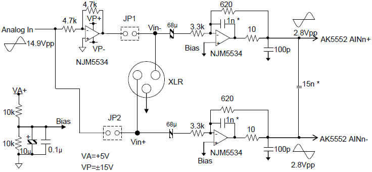
Example
We have equations, so we can design our filter.
We want a LPF filter with flat frequency response for an ADC, so the quality factor is 0.707. The cutoff frequency is 370 kHz to have the frequency response smooth over the audio bandwidth. The ADC input voltage is 2.8 Vpp and the maximum input voltage is 14.9 Vpp.
Choose the feedback R2 value, for example, 620 Ohm, and the R3 value, for example, 10 Ohm. Now we can calculate the other component values.
           1                              1
C1 = ————————————— = —————————————————————————————————————————— = 966 pF
     (R2 + R3) Q ?   (620 Ohm + 10 Ohm) ? 0.707 ? 2 ? ? 370 kHz

     (R2 + R3) Q      (620 Ohm + 10 Ohm) ? 0.707
C2 = ——————————— = ———————————————————————————————— = 30.9 nF
       R2 R3 ?     620 Ohm ? 10 Ohm ? 2 ? ? 370 kHz

     R2   R2 Vin   620 Ohm ? 14.9 V
R1 = —— = —————— = ———————————————— = 3299 Ohm
     A     Vadc          2.8 V
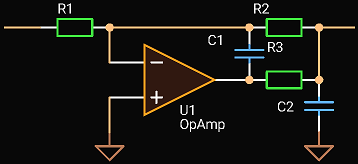
We see this circuit as the input filter in the AK5552 datasheet from Asahi Kasei, but since C2 is connected across the differential output its value is divided by 2. C2 is split into 3 capacitors, 100 pF capacitors are used to filter common-mode signal and their value about 100 times lower than the differential capacitance which prevents common-mode noise from being converted into differential noise due to component tolerances. A Fully Differential Amplifier can be used here too.
 |
| AK5552 input low-pass filter |
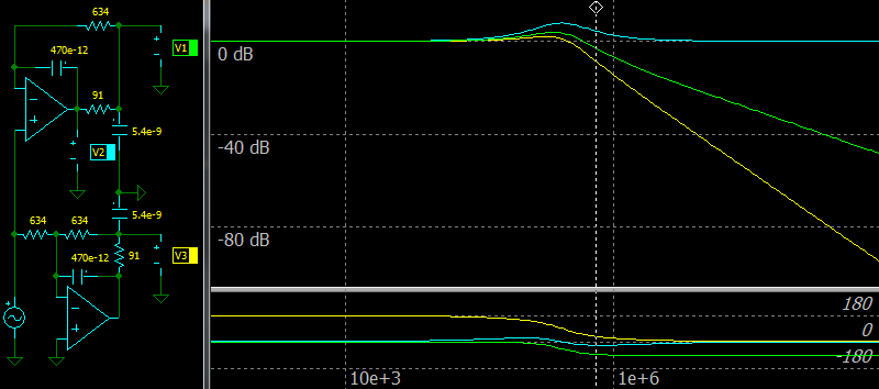
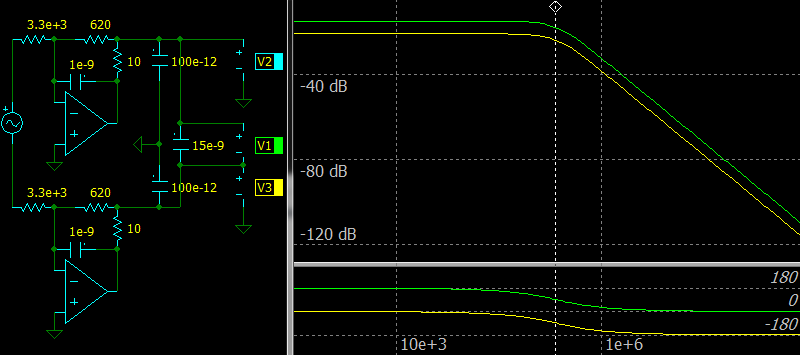 |
| AK5552 input low-pass filter, simulation using ideal Op Amps |
The frequency response is smooth and meets expectations.
Similar circuits
Let’s look at datasheets of other vendors.
Cirrus Logic
 |
| CS42528 input low-pass filter |
The analog input buffer in the CS42528 datasheet look familiar, but still there is some difference in the top amplifier connection.
Let’s write transfer functions of the circuit for the AINL1+ output and the Op Amp output:
 |
                      1 + C1 (R1 + R2) s                 1
AINL1+(s) = —————————————————————————————————————— ? —————————
            1 + C1 (R1 + R2) s + (C1 C2 R1 R2) s^2   1 + s / ?
It does not look like the 2-nd order low-pass filter transfer function! It looks more like a 1-st order filter and the transfer function is also similar with a 2-nd order band-pass filter prototype:
               s / (Q ?)
H(s) = —————————————————————————
       1 + s / (Q ?) + s^2 / ?^2
So we can wait slope of ?6 dB/octave and some peaking is possible.
In fact, it is two filters in one, a low-pass and band-pass:
                   1                       s / (Q ?)
H(s) = ————————————————————————— + —————————————————————————
       1 + s / (Q ?) + s^2 / ?^2   1 + s / (Q ?) + s^2 / ?^2
Thus we can estimate that some kind of the «cutoff radial frequency» (not a peak frequency, because it is still close to a low-pass filter and not a band-pass) is:
          1
? = ——————————————
    v{C1 C2 R1 R2}
the «quality factor» is:
    v{C1 C2 R1 R2}
Q = ——————————————
     C1 (R1 + R2)
Very similar to the first circuit, right?
Now let’s evaluate the signal at the Op Amp output.
         1 + (C1 (R1 + R2) + C2 R2) s + (C1 C2 R1 R2) s^2
Out(s) = ———————————————————————————————————————————————— ? 1
              1 + C1 (R1 + R2) s + (C1 C2 R1 R2) s^2
Out(s) looks like just an amplifier because all terms look similar.
We can find a similar circuit in [2], Chapter 6, Figure 6-74, where it is used for active capacitive load compensation.
Use a simulator to see signals at both points.
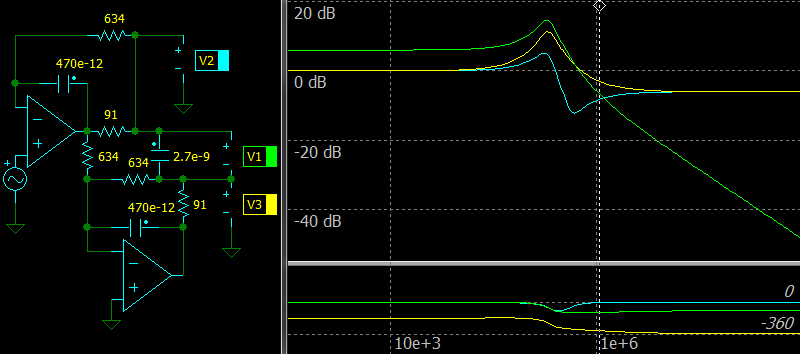
 |
| CS42528 input low-pass filter, simulation of both legs using ideal Op Amps |
The top circuit is the top leg of the input differential filter and the bottom circuit is the bottom leg. Although both circuits look similar, they operate in different ways. The green line shows the top leg output which has the slope of ?20 dB/decade, so it is mainly a 1-st order filter, while the yellow line of the bottom filter output has ?40 dB/decade and it is a 2-nd order filter. The cyan line is the top Op Amp output used as the input of the bottom cascade.
Let’s use our equations and compare them with the simulation.
                   1                               1
Fcutoff = —————————————————— = —————————————————————————————————————————— ? 416 kHz
          2 ? v{C1 C2 R1 R2}   2? ? v{470 pF ? 5.4 nF ? 634 Ohm ? 91 Ohm}

    v(C1 C2 R1 R2)   v(470 pF ? 5.4 nF ? 634 Ohm ? 91 Ohm)
Q = —————————————— = ————————————————————————————————————— ? 1.123
     C1 (R1 + R2)         470 pF ? (634 Ohm + 91 Ohm)
There is a peak at about 392 kHz, ?3 dB frequency is about 735 kHz.
Now it is interesting to see the final result when they are connected as in the datasheet.
 |
| CS42528 input low-pass filter, simulation |
It looks quite strange, isn’t it? The differential roll-off exists due to changes in phase shift between output signals. The basic idea was to have a high impedance buffer using the non-inverting version of the filter. The response is still smooth over the audio bandwidth.
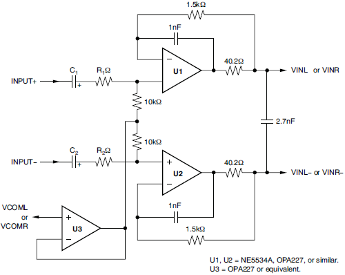
Texas Instruments
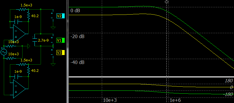
Looking at the PCM4222 datasheet we see two variants of the analog input filter.
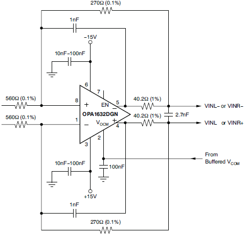 |
| PCM4222 input low-pass filter using fully differential amplifier |
Let’s reverse its parameters:
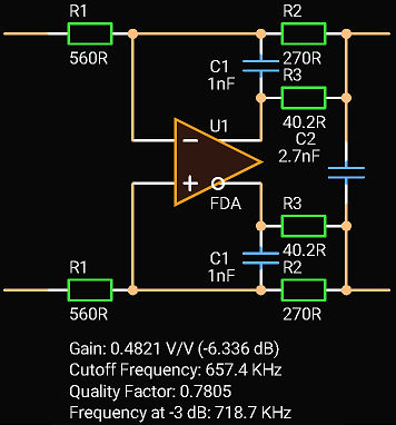 |
| PCM4222 input low-pass filter reversed |
They use quality factor that causes some peaking and twice the bandwidth.
 |
| PCM4222 input low-pass filter, frequency response with ideal amplifier |
We know that the non-inverting variant of the circuit acts like a 1-st order filter with some peaking. Let’s look how Texas Instruments’ engineers solved this problem.
 |
| PCM4222 non-inverting input low-pass filter |
 |
| PCM4222 non-inverting input low-pass filter, simulation using ideal Op Amps |
The frequency response is quite smooth over the audio bandwidth, ?3 dB frequency is about 855 kHz, though there is a peak about +0.5 dB at about 177 kHz. The slope is ?20 dB/decade.
                   1                                  1
Fcutoff = —————————————————— = ——————————————————————————————————————————————— ? 279 kHz
          2 ? v{C1 C2 R1 R2}   2? ? v{1 nF ? 2 ? 2.7 nF ? 1.5 kOhm ? 40.2 Ohm}

    v(C1 C2 R1 R2)   v(1 nF ? 2 ? 2.7 nF ? 1.5 kOhm ? 40.2 Ohm)
Q = —————————————— = —————————————————————————————————————————— ? 0.37
     C1 (R1 + R2)           1 nF ? (1.5 kOhm + 40.2 Ohm)
Design of active «in-the-loop» capacitive load compensation circuit
Let’s check our ideas and design our non-inverting input buffer with a capacitive load.
Let the «cutoff frequency» be 100 kHz and “quality factor” 0.1 to minimize peaking.
A capacitive load is
          Q R2                     0.1 ? 100 Ohm
R1 = ——————————————— = —————————————————————————————————————— ? 45.3 Ohm
     2 ? F C2 R2 ? Q   2 ? ? 100 kHz ? 5.1 nF ? 100 Ohm ? 0.1

              1                                 1
C1 = —————————————————— = —————————————————————————————————————————————— ? 0.1 uF
     (2 ? F)^2 R1 R2 C2   (2? ? 100 kHz)^2 ? 45.3 Ohm ? 100 Ohm ? 5.1 nF
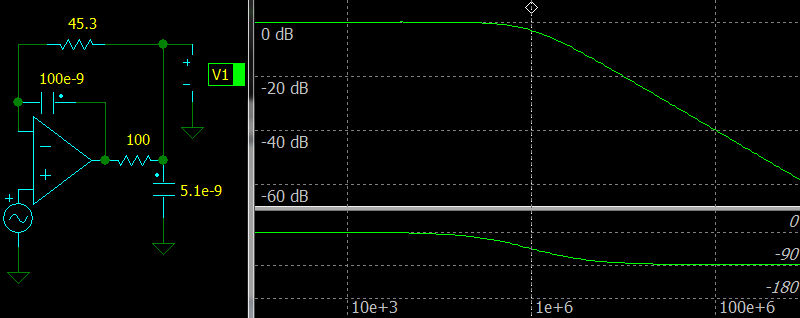 |
| Active «in-the-loop» capacitive load compensation circuit, simulation |
There is just a really small peak of +0.08 dB at about 40 kHz, but ?3 dB frequency is about 1 MHz, so if we need a lower corner frequency, the “cutoff frequency” must be changed. Component values can also be varied to find suitable ones.
More equations for more accurate circuit design.
                         F?3dB Q v2
Fcutoff = ———————————————————————————————————————
          v{v{4 Q^2 (2 Q^2 + 1) + 1} + 2 Q^2 + 1}
The peak in times:
                      (Q^2 + 2)^(1/4)
? = ————————————————————————————————————————————————————
    v{2Q^3 (Q^2 + 2) + (1 - 2 Q^2 (Q^2 + 1)) v[Q^2 + 2]}
The frequency at ?3 dB:
        v{v{C1^2 (R1^4 + R2^4) + 2 R1 R2 [2 (C1 + C2) (C1 (R1^2 + R2^2) + 2 C2 R1 R2) + 3 R1 R2 C1^2]} + C1 (R1^2 + R2^2) + 2 R1 R2 (C1 + C2)}
F?3db = ——————————————————————————————————————————————————————————————————————————————————————————————————————————————————————————————————————
                                                               2 ? C2 R1 R2 v{2 C1}
The frequency at a peak:
        v{v{C2 R1 R2 [2 C1 (R1 + R2) (R1 + R2) + C2 R1 R2]} / (C2 R1 R2) - 1}
Fpeak = —————————————————————————————————————————————————————————————————————
                                2 ? 2 C1 (R1 + R2)
Conclusion
Both topologies are suitable for analog input buffer for ADC, but only the inverting version is a second order low-pass filter.
The advantages of this filter topology are:
- The capacitor at the output. It acts like a hold cell that is suitable for ADC, and compensates frequency dependent output impedance of a compensated Op Amp;
- The DC gain can be changed by replacing only one resistor and can be greater or lower than 1;
- An Op Amp and Fully differential Amplifier can be used in this topology;
- A constant and active input impedance over the frequency range;
- The output voltage can have a DC offset, so it can be used in single supply circuits or with single supply ADCs;
The disadvantages are:
- Quite low input impedance and inverting output;
- An Op Amp must be able to work with capacitive load;
It is interesting that this filter type is used only as an input buffer for ADCs and not used after DACs. There is a deep studying of low-pass filters design in [3], Chapter 10 and 11, for Sallen-Key and Multiple-Feedback low-pass filters. Maybe there are some hidden disadvantages in this topology? Or is it just that not all engineers know about this topology or are afraid to use it?
References
- Analog Devices. “Linear Circuit Design Handbook”. Chapter 8, “Analog Filters”.
- Analog Devices. “Op Amp Applications Handbook”. Chapter 6, “Signal Amplifiers”.
- Texas Instruments, “Active Low-Pass Filter Design”.
- Asahi Kasei, AK5552 datasheet.
- Cirrus Logic, CS42528 datasheet.
- Texas Instruments, PCM4222 datasheet.
- «idealCircuit», a simulator.
- «Filter Designer», a multistage analog active filter design tool.
- «Circuit Calculator», an electronics circuit design tool.