Passcode Data Protection by Using FPGA and Verilog
Authors
Artem Murashko, Makar Shevchenko and Artem Chernitsa.
Introduction
There are many situations when you need to protect your data, and different tools can be used to do that. For example, a safe. We develop a passcode data protection mechanism by using an FPGA board and Quartus Prime software. It allows demonstrating the basic concepts of a combination lock such as entering data, setting and checking a passcode, and displaying data.
Hardware and software used
Our project is implemented by using following devices and technologies:

Cyclone IV FPGA Device
? Buttons (input device)
? LEDs and 7-Segment display (output device)
? Power Supply port (used to power FPGA board)
? USB Blaster connector (used to upload firmware)
Quartus Prime Lite Edition 18.1
? Verilog HDL
Altera USB Blaster (USB Blaster transfers configuration data from PC to FPGA)
Technical implementation
Schematic representation of program execution
The diagram in Figure 2 shows the flow of the program. The circles are states, arrows are transition conditions.

Displaying the state of the program
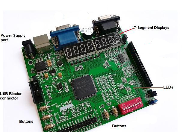
We used LEDs to display the current state of the program. Cyclone IV FPGA board have 12 LEDs and each LED has its own number. Figure 3 shows the LEDs arrangement.

D4 to indicate the state "Enter data to be saved"; D7 to indicate the state "Set up the passcode"; D10 to indicate the state "Enter the passcode"; D13 to indicate the state "Show data has been saved";
?
7-Segment display
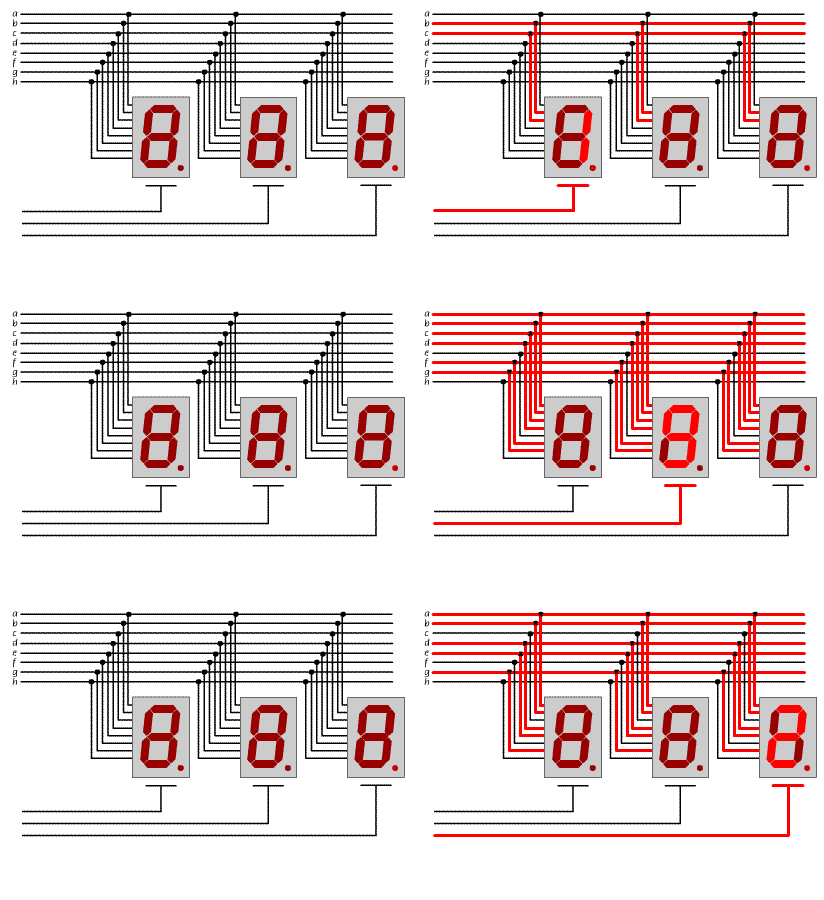
If we want to bind each cathode (stick) to the registers, than it would take 8*8=64 power tracks for each display. To save space on the board, the display developers decided to connect all the displays together. Therefore, if we want to light up element 'C' on the display, then after applying power, all elements of 'C' will light up. Figure 4 shows the individual segments of a display.

Figure 4: The individual segments of a display. The solution to this "problem" is very simple, we need to quickly switch between displays, lighting the necessary elements. This process is shown in Figure 5. The question comes up, with what frequency should we do this? By default, each FPGA has a clock generator that serves as a tool for synchronizing operations. On Cyclone IV, it operates at a frequency of 50 MHz. But if we switch displays at this speed, we will not have time to see the LED updates, and all displays will have the same combination. After experimenting, we came to the conclusion that the optimal refresh rate of the indicator is the FrequencyOfClock / (5*10^4) ? 10^3 updates per second.

Figure 5: Quick switching between displays. Buttons
The problem is called "button bounce". Button click occurs at an arbitrary time, therefore, relative to the rest of the circuit inside the FPGA, it is an asynchronous event. The change of the logical state on the input leg of the FPGA can coincide with the moment of switching the receiving trigger, and there is a possibility that the trigger will be in an undefined ("non-digital") metastable state. Figure 6 shows the scheme of the key bounce.?

The solution is to differentiate stable signals from false alarms using timer. You can read a detailed solution here.
Demonstration
Step-by-step instruction
Here is the step-by-step instruction, how to get the same result:
1. Install Quartus Prime 18.1
2. Open Quartus Prime 18.1

3. New project wizard
4. Press "Next" (This section may not be displayed if you disabled it earlier).
5. Choose directory for your project, set some name for project, set "top" as top-level entity. Press "Next" (Directory, Name, Top-Level Entity).
6. Select "Empty project". Press "Next" (Project type).
7. Press "Next" (Add Files).
8. Firstly, choose your device family in "Family" list. Secondly, select your device in the "Available devices" list (Usually device name is written on FPGA, in other words, on big black square). Finally, press "Next" (Family, Device & Board Settings).
9. Press "Next" (EDA Tool Settings).
10. Press "Finish" (Summary).
11. Create all files and copy paste corresponding code from GitHub repository using following approach: File -> New -> Verilog HDL -> OK -> copy paste the code -> File -> Save as... -> set corresponding to code name -> Save
Here in README.md we placed description of the code
12. Processing -> Start Compilation -> Wait for compilation to be finished

13. Assignments -> Pin planner.
14. Now let's assign pins to the inputs and outputs of the top module. You should examine the inscriptions on your board.

Set the following pins for the anodes:
- anode[0] — pin of BIT0 (most right digit)
- anode[1] — pin of BIT1
- ...
- anode[7] — pin of BIT7 (most left digit)
- button_increase — pin of some button 1. This button will increase selected digit.
- button_left — pin of some button 2. This button will shift selection to more left digit.
- button_next — pin of some button 3. This button will move to the next state of the combinational lock.
- cathode[0] — pin of A cathode
- cathode[1] — pin of B cathode
- ...
- cathode[7] — pin of H (DP) cathode
- clk — pin of CLK_50M(it could have different name of your plate, important that it should contain part "CLK")
- lights[0] — pin of some light-emitting diode 1. It will indicate state 1
- lights[1] — pin of some light-emitting diode 2. It will indicate state 2
- ...
- lights[4] — pin of some light-emitting diode 5. It will indicate state 5
Pin planner will looks like that:

15. Close Pin planner.
16. Tools -> Programmer -> Hardware setup -> Select your device (if you do not see it, make sure that you connected device to your PC and installed drivers for it. We installed drivers using this guide)
17. Close Hardware setup.
18. Press Start.
19. Done, combinational lock installed on your device!
Conclusion
We described the key implement stages of a passcode-protection mechanism by using an FPGA board, Quartus Prime software and Verilog hardware description language. This work has been implemented in the scope of «Computer Architecture» course in the Innopolis University. The proposed implementation can be extended for usage in the industry application and for education process.
Acknowledgments
The authors would like to express gratitude to our professors Artem Burmyakov, Muhammad Fahim, Alexander Tormasov and to our teacher assitant Vlad Ostankovich for giving us deep knowledge and possibility to use it in practice.
References
? [1] Project on the GitHub
? [2] Debouncer using Verilog
? [3] FPGAs For Dummies

